Material Anlysis
Electron Microscopy and EELS analysis
Transmission Electron Microscopy, TEM
The high spatial resolution of transmission electron microscopy makes it become one of the most important analyzing tool in materials research. According to the interaction between electrons and specimen, information provided by TEM can be divided into three kinds. (1) Image, it is formed by using transmitted electron or elastic scattering electron. (2) Diffraction pattern (DP), it can be used to investigate microstructure and crystal structure. (3) To identify composition and chemical bonding by using EDS and EELS equipped with TEM.
The spatial resolution of TEM is better than that of X-ray analysis. In 1950s, line defect and planar defect can be detected by TEM. Nowadays, the spatial resolution has been improved to atomic level, which makes it easier to derive information from materials. Includes the variations within unit cell (point defect), crystal structure of compound, arrangement of atoms at grain boundary and interfaces, etc. can be investigated by using TEM analysis.
Electron Energy Loss Spectrum, EELS
EELS measures the distribution of energies lost by an energetic electron (typically 100 ~ 1000 keV) as it passes through a thin solid specimen (typically 5 ~ 500A?). The energies loss comes from electrons that have interacted inelastically with the specimen. These collisions tell us about the electronic structure of the specimen atoms, i.e., the bonding and nearest-neighbor distributions and the dielectric response. A typical electron energy loss spectrum, recorded from a thin specimen over a range of about 1000 eV. It consists of zero- loss, low- loss (plasmon- loss) and core- loss regions. Characteristic features (ionization edges) in the EELS spectrum offer an alternative means of identifying and quantifying the elements present. The near edge fine structure (ELNES) and extended energy loss fine structure (EXELFS) provide further information about the local density of unoccupied electronic states at the exited atom in the solid, thus additional information on phases, bonding and electronic structure can be obtained. X-ray absorption spectroscopy (XAS) also provides similar information to EELS. Specimens can be examined in a gaseous environment or even fully hydrated. However, the spatial resolution of XAS is not as high as that of EELS. Combined EELS with the high-angle annular dark-field imaging (HAADF) or Z-contrast imaging in STEM, it is possible to measure the composition and obtain electronic structure information with a spatial resolution down to an atomic level.
Follows are some results we use TEM and EELS to investigate materials with superconducting or magnetism.
|
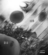
Figure 1. TEM result of SmBCO material.? In addition to the continuous superconducting phase (123) and non-superconducting particles (211), there are many defects and twins in the matrix. |
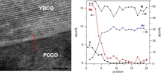
Figure 2. TEM/EDS results of YBCO/PCCO bilayers. Left figure shows the high quality film with layered structure. The interface between these two phases is quiet sharp. EDS result, as shown in right figure, indicates that the inter-diffusion at interface is unobvious. |
|
|
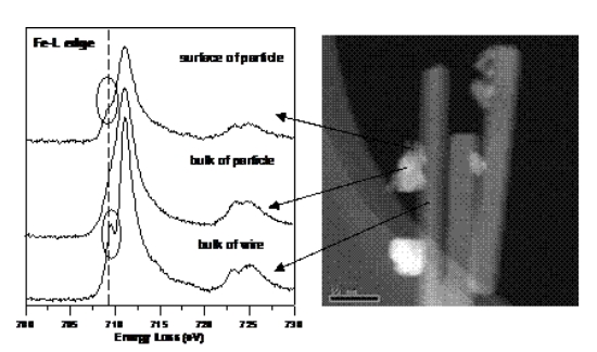
Figure 3. Phase identification of iron-oxide by using STEM/EELS. According to the fine structure (ELNES) of spectrum, the valance of iron can be identified. The results indicate that in the particle, the valance of iron is a mixture of 2+ and 3+. At surface of particle, the fraction of 3+ is higher. On the other hand, the valance of iron is 3+ of the wire. |