Scanning Tunneling Microscope(STM)
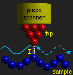
STM was invented by Gerd Binnig and Heinrich Rohrer, who sequently received Nobel Prize in physics in 1986 for their achievement. In a STM, a very sharp metal tip is brought very close to the sample surface without physical contact. As an electrical bias voltage is applied to the sample, the electrons tunnels through the vacuum barrier. The tunneling current depends on the tip-sample distance exponentially; i.e. 0.1nm change in tip-sample distance results in a 10 times difference in tunnel current. By precisely measuring this current at different location and controlling the tip-sample distance, we can image the sample surface with high spatial resolution.
Spectroscopic imaging by STM
(1) Topography
In this mode, a feedback loop is used to keep the tunnel current constant by adjusting the tip-sample distance with a piezo scanner. The adjustment (the voltage applied to the peizo scanner) is recored as function of location (x, y), which represents the relative variation in height of the sample surface, assuming no change in local density of states (LDOS).
(2) Scanning tunneling spectropy (STS)
The differential conductance, dI/dV at an energy of E=eV is proportional to LDOS(E) of the surface in an ideal case. By measuring dI/dV at the energy range of interest, we can obtain the dI/dV spectrum at a given location (x, y).
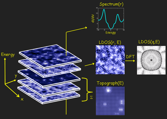
(3) Differential conductance map, dI/dV(x, y, E) and Fourier transform-STS
By taking the differential conductance, dI/dV(E) as function of location (x, y), a 3D map of LDOS(x, y, E) can be obtained and reveals the spatial variation of electronic structures with atomic resolution. In addition, the standing waves of quasiparticle interference, resulting from quasiparticles scattering off impurities or defects, can be measured by Fourier transform of LDOS map. This technique yeilds the key information on the electronic truncture in momentum space.
Our home-built spectroscopic-imaging STMs (SI-STMs)
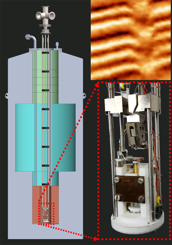
It takes several days to acquire one spectroscopic map. Moreover, it is necessary to keep register to the same field of view with atomic precision when we change the experimental condition such as temperature or magnetic field. To achieve such conditions, the design of our STM system has to reach the ultimate mechanical stability.(1) 1.5K-9Tesla UHV SI-STM
The picture below shows our first home-built SI-STM system inside a NIC-56 soundroom, which can greatly reduce the acoustic noise. For our homemade vibration isolation system, three large heavy pillars (each is filled with ~500kg lead) connect to form a stable tripod structure. Three pneumatic isolators with neutral frequency of ~1Hz are mounted on each pillar to support a lead-filled table (~900kg), where our STM system is installed. The homemade cryostat has a cleaving mechanism so we can cleave the single crystal at T < 20K in UHV. The Pan-type STM head is mounted on a home-made low vibration 4He pot refrigerator, which can achieve the base temperature ~ 1.5K at the STM head. The system is fitted with a custom-made 9 Tesla magnet dewar. The helium boil-off rate is ~4.8 L/day, which allows us to take spectroscopic maps continuously for ~10 days.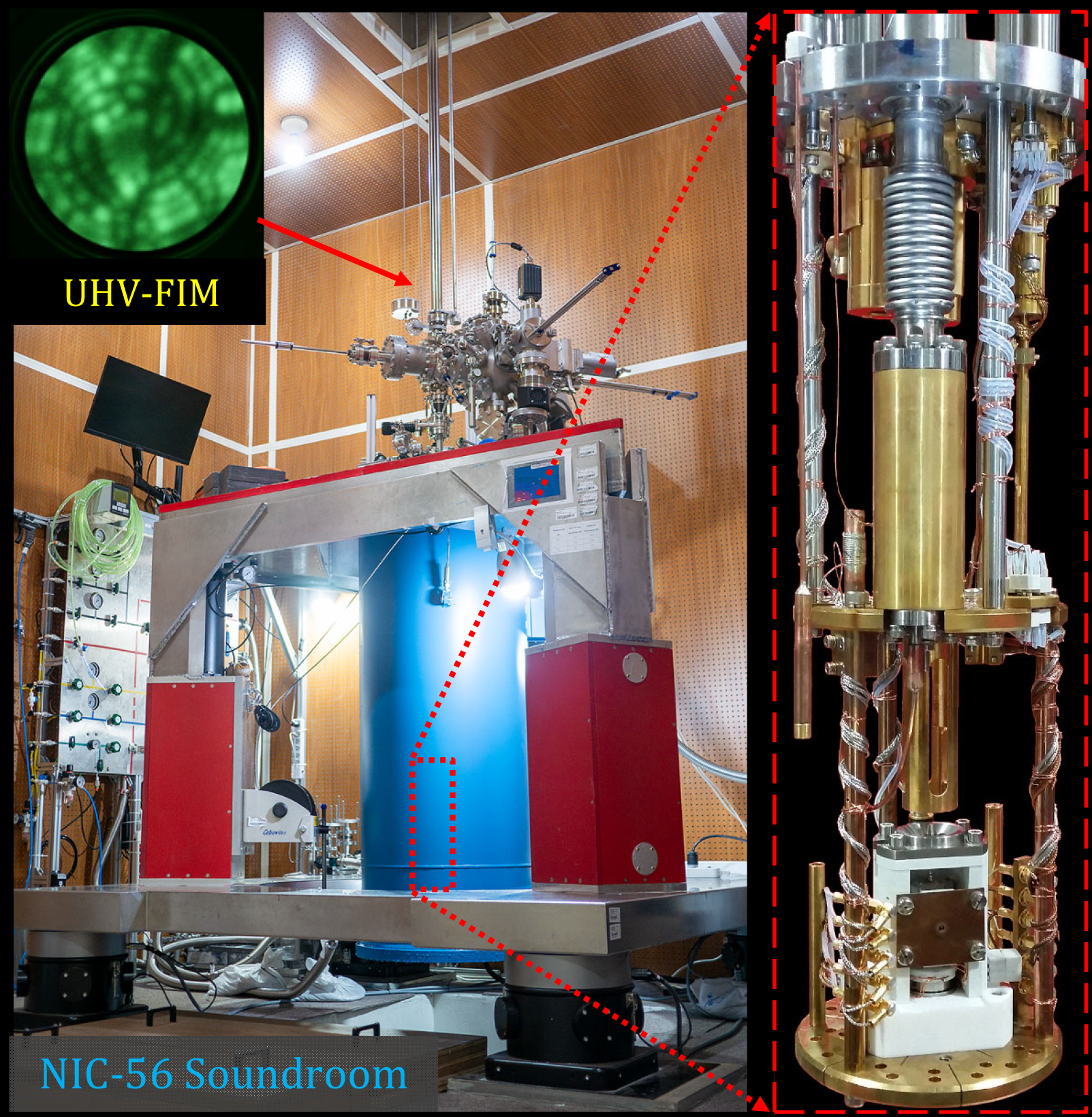
(2) 300mK-16Tesla SI-STM and the Precision Measurement Lab
The second is our new 3He-SI-STM as depicted below. The system is installed in the Precision Measurement Lab inside the Interdisciplinary Research Building at Academia Sinica. The Precision Measurement Lab is specially designed for ultra-sensitive experiments like SI-STM. The lab floor is a 75ton concrete block that is decoupled from the main building floor by a thick layer of sand. We further installed our homemade vibration isolation system to minimize the vibrational noise. The lab is acoustically shielded and temperature/humidity regulated so that the environmental impact on the measurements is minimized. We can now operate this SI-STM system for ~7 days at T~270mK and reach the energy resolution of ~110µeV. Combined with the 16Telsa magnetic field, our 300mK-16Tesla SI-STM is not only the first in Taiwan but also unique in the world.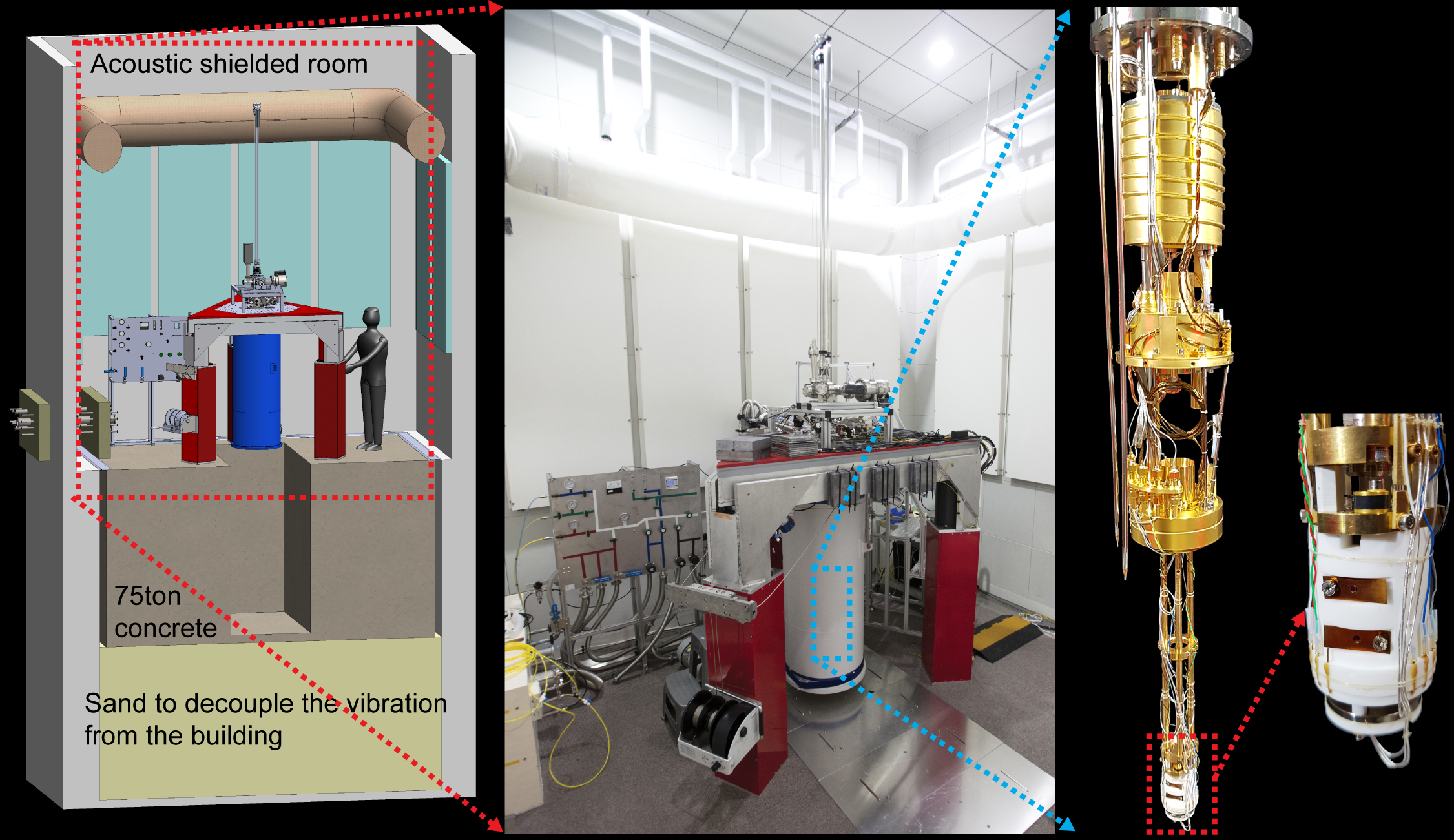
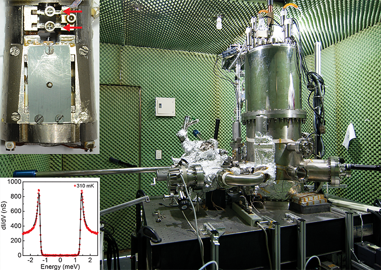
(3) 3He-7Tesla UHV STM System
We collaborate with Dr. Chia-Seng Chang to retrofit and to improve the overall performance of this existing 3He UHV STM system (figure below). This system consists of a UHV preparation chamber and load-lock chamber, which enables us to transfer/prepare the tip and the sample between different UHV chambers. A double stage 4He-3He sorption cooler is used to cool down the STM head to T ~ 280 mK with the holding time ~ 24 hours by pumping the liquid helium reservoir and then the 4He pot. Such a fridge design is vibration ¡§free¡¨ because closed-cycled sorption pumping does not generate vibration. The electron temperature is determined to be ~400mK by fitting the measured superconducting gap (the bottom inset). Furthermore, we retrofit a novel double-deck sample stage on the STM head (the top inset), which gives us a simple way to clean the STM tip or to prepare a magnetic tip for spin polarized STM. Also, the original sample can be preserved in the STM head so the comparison can be made on the same field of view.Further information can be found in Ultramicroscopy 196, 180 (2019)
Low temperature scanning force microscope
While STM is a powerful technique to study the electronic properties of quantum materials, its application is limited to conducting samples. Gerd Binnig, Calvin Quate and Christof Gerber invited the scanning force microscope (SFM or often called atomic force microscope, AFM) in 1985 so that one can visualize both insulating and conducting samples with similar spatial resolution. Since then, SFM has been developed to reach the true atomic resolution and to measure a wide range of tip-sample interactions such as magnetic force and electrostatic force. Nowdays, commercial SFMs can be seen in many laboratories. However, most of them can only be operated in room temperature and in the absence of magnetic field. Here, we develop a SFM that can be operated between T = 4.2K to room temperature and under a magnetic field up to 9T (vertical) or 1T (horizontal). The cantilever deflection is measured by a fiber-optic interferometer, which allows us to use many different tips that are commercially available.